In September 2020 I decided to stop working for the first half year of 2021 and go back to studying. I had just applied for the Fab Academy, a globally run, full-time course of 20 weeks, headed by Neil Gershenfeld from MIT, focused on learning how to become a maker / fabricator. Making designs on a computer and then turning these into a reality with machines such as laser cutters, 3D printers, milling machines, and more, while also incorporating electronics. It’s also known as “How to Make (almost) Anything”.
Seriously, during some weeks I didn’t even have time to get groceries!
Some of the weeks were the most intense I’ve ever experienced in terms of workload. Basically all of the weeks were very rewarding in what I learned and made. And almost all of them were extremely fun as well (I’ll get to casting later ( ̄ー ̄) ). Otherwise I would’ve never been able to keep working those insane hours (big disclaimer; I did this to myself, others managed to pull it off while continuing to work, but their weekly assignments were generally a bit simpler then).
While I was investigating if the Fab Academy might be something for me, I found it hard to truly get a sense of what the topics of each week implied. There’s a schedule that gives each week a name. But as a true newbie in the world of fabrication, I had no idea what Electronics Design and Electronics Production really were (and what the difference even was), or how Computer-Controlled Machining wasn’t the same as Computer-Controlled Cutting. I figured it might therefore be helpful if I wrote a little about the whole experience and show, in a nutshell, what topics came to pass, what they meant, and what I created during each week.
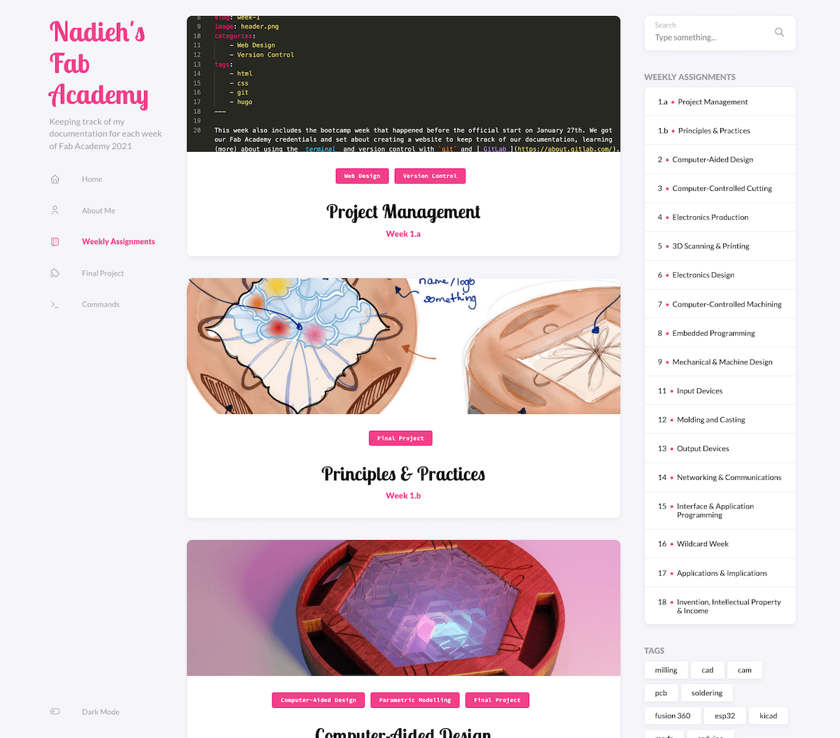
I’ve written ridiculously extensive posts about what I did and learned during each week of my Fab Academy on a dedicated website, which you can find here.
My Reasons for Applying
You (generally) don’t just decide to stop working for six months, thereby having no income, when you wake up one day. I therefore wanted to explain in a bit of detail my reasons, doubts, and final motivations for choosing to do so, because I’ve had people ask me about it while I was going through the weeks and sharing results online. If you’re not interested, you can skip this whole section.
Fab Academy had come onto my radar during the start of 2020. I was still very much enjoying my work to create data visualizations. However, I was getting more and more intrigued to learn how to take my designs away from the digital and into the physical world.
At the start of the pandemic I bought an AxiDraw A3/V3 pen plotter, with which I thoroughly enjoyed myself for a while. Having virtually no clients, I could create the mental space to create spirograph and other mathematically driven designs for it.
I wanted more! I searched for workshops near Amsterdam in silkscreen printing, riso printing, laser cutting, 3D printing, etc. Through this search I found the website of the Waag, the oldest (non-religious) building in Amsterdam, which houses a so-called FabLab. These labs can be found all over the world and are places where you have access to different kinds of machines, generally computer-controlled, to create tangible things. Looking for a workshop I instead found the Fab Academy page and was immediately intrigued. The thought of being able to immerse yourself into the whole process of fabrication for almost 6 months sounded awesome. But the 2020 FabAcademy was already underway, so I made a reminder for September to check it out again and perhaps sign up for the 2021 cycle.
September came around and the reminder popped up one day. I was still very intrigued, but damn, six months without income? I wasn’t sure it would be that valuable. Nevertheless, no harm in at least learning more. I reached out to the lab instructor of the Waag, Henk, and we set up a day where I could come by and have a chat about all things Fab Academy. I definitely left that conversation being even more enthusiastic.
I truly had (and still have) no idea how I’m going to use the skills from the Fab Academy in my daily work. Everything that I create is made with code, but never consists of anything tangible, apart from a print. I would love to make a dataviz installation, for sure, but that’s not the type of client that finds me. I could therefore not really make “a case of ROI” for myself. However, after letting it simmer for a few more days, I decided that it just felt right. It felt like I feel when having just thought of a great subject to do for a personal project. That kind of “I can’t wait to start”-enthusiasm. The prospect of increasing my knowledge horizon in so many new areas, who knew, sometimes you first need to take the step before a (monetary) benefit could come from it that I wasn’t aware of yet. But more importantly, even if it never resulted in new knowledge/skills that I could use for my work, I realized I would still be ok with that.
I was grateful that I’d been able to save enough money to bridge a 6-month gap. And why only stop working when you retire? I still have about 35-ish years to go, I figured I could take a “sabbatical” when I’m 34 (although this was noooo vacation).
And thus I applied.
The General Weekly Setup
Let me explain this in some detail as well, because I wasn’t able to find much info about how a typical week looked when I was investigating Fab Academy.
Weeks run from Wednesday to Wednesday, starting at 10:30am Boston time (those poor students in Asia that end up having class at the middle of the night ಥ_ಥ ). I personally think it’s this way because then you’re basically using the weekend to make your designs, being able to spend 7 effective days on each week, versus going from Monday to Monday. You learn about the new technique and tool on Wednesday/Thursday/Friday, make your design on Friday/Saturday/Sunday, create and iterate on Monday/Tuesday, present on Wednesday. But that’s just a “this is my experience” guess (*^▽^*)ゞ
My gosh, I’ve never experienced someone who knows this much and is as smart and knowledgeable as Neil. He never ceased to amaze me.
From 10:30am Boston time on Wednesday, Neil Gershenfeld, who began and leads the Fab Academy (and the overarching Academany) gives a ±1.5 hour lecture on the topic of the week. This is truly a fly-by of everything that you could/should possible know. It’s too much to wrap your head around if the subject is new. It’s fascinating though, and a treasure trove of information.
From discussing machines that normal people can buy to those that cost millions of dollars. Talking about parts, materials, vendors. But also techniques, what you should and shouldn’t do to get a better result, safety! (some of the machines can be lethal if not operated with care, truly). Living near Amsterdam, this class ran from 16:30 - 18:00 each Wednesday, which I watched from home, while sharing some thoughts with my 7 fellow students at the Waag over the chat. Afterwards it came down to decompressing that intense 1.5 hour, but generally waiting for Thursday to do anything with it.
On Thursday I and my fellow students at the Waag would go to the lab where we would get the “this information you can grasp” version of Neil’s lesson from our local lab instructor (Henk). He would talk us through the most important points, sometimes with slides, and afterwards explain how the machine worked, how to operate is safely, and showed some tests.
After these instructions we got a group assignment. This generally comes down to figuring out for ourselves (as a group) what the limits of the machine are; How thin is the laser beam that cuts away just a bit of the material? What are the smallest traces you can mill on a copper plate? What is the lowest angle you can 3D print at without the filament drooping? Play with as many sensor devices as you can. We always managed to finish this group assignment before the end of the day.
The rest of the week (from Friday to Wednesday) you basically have to work on your weekly individual assignment. This slowly morphs into working on your final project during the final few weeks. It always starts with a design made on the computer. Either a 2D or 3D model, or a electronics design to make your own circuit board.
Generally I would work on my design over the weekend and on Monday/Tuesday I would be using a machine to create it. Often that wasn’t perfect on the first (or second) go and I’d have to make adjustments and try again, if time and machine availability allowed. Sometimes I was lucky and could already do a quick test on Friday, so I could fine-tune the design during the weekend.
Henk’s motto was “read the f&*ing manual”
Throughout this all we could ask our lab instructor Henk for advice or thoughts on how to go about things. Although he could be downright grumpy at times, he always wanted to see the students succeed, but he wasn’t going to hold your hand. You had to try and figure stuff our yourself, but he’d freely supply tips, share knowledge that we needed but didn’t yet have (e.g. a component that would do exactly what we needed), or fix machines pronto if you’d messed up (we did… a lot…) so we could continue as fast as possible.
You have no idea how often I found myself digging through documentations of previous students when the electronics and programming weeks came by.
And then there’s the DOCUMENTATION!! Documenting every. step. of. the. way. is a fundamental pillar of Fab Academy. It’s what makes you be able to graduate. You have to document and explain how to operate the machines (e.g. what button does what), how you did the group assignment, how you designed your weekly (and final) project, definitely what mistakes you made (and how you maybe solved them), and how you made your weekly assignment. Part of this is to show the instructors and FabAcademy global that you have learned the skills, part is to have as a reference manual for the upcoming weeks when you’ll be using the machines again, and part is to help future students out when they get stuck on something that you also got stuck on and eventually solved. As an example you can take a look at the write-up of my Computer-Controlled Cutting week.
I use many words to write (as you may have noticed). I’d say that I spent 40% - 50% of my time on Fab Academy documenting. A lot of time. It really was “a day in the lab/a day of design, a day documenting”. This percentage dropped a little during the final weeks when I didn’t have new machines to write about. In all honesty though, I have been told that nobody has ever written longer weekly write-ups than I have, in the history of Fab Academy since 2008…(I think the first was in 2008?) An interesting honor to have, hehe. I therefore think that generally the percentage is lower for other people.
At noon on the Wednesday we would have a wrap-up call with Henk and all the students at the Waag. Looking back on the week and looking ahead to the next one. Between 13:00-14:00 we would have a regional meeting with a few more labs (in Germany, Belgium and France), during which we talked everyone through what we experienced and made in a few minutes each. I quite liked these regional reviews, because you’d get to see what other people had been working on, expanding my views on what was possible. Finally, from 15:00 - 16:30 Neil would do the global review during which students are chosen by a randomizer to talk Neil through their work from the past week (using the documentation), and talk him through your final project ideas during which he’ll give recommendations on ways to go about it.
A note about those reviews directly with Neil. There’s basically really no way you could have done anything wrong with what you did. He’s not grading you, mistakes are good, as long as you tried. BUT, if your documentation isn’t extensive enough, you will get a stern remark to update it and do better. (A nice result though is that when you’ve had your global review with Neil once, you’ll never be picked again, so you can relax a little during all the next global reviews).
You will need to finish the requirements of each weekly assignment to graduate though (you can find them all here). However, it’s fine if you finish it during later weeks (or even after the official 20 weeks, then you’ll just officially graduate in the next year).
And that’s where the week ends and starts all over again for the new topic.
Week 1a | Project Management
On January 27th the first week officially started. And this was no “gentle startup”. The goal was to create our Fab Academy page for the documentation. If you’ve never programmed before that came down to learning the basics of using a terminal, using git, HTML, CSS and markdown, at the very least.
Sure, Fab Academy provided everyone with a default template to use for their website. But really, who wouldn’t want to make something that’s more personal and unique, for that time that your number gets called during the global reviews right? (But it was of course fine to stick with the template, which many also did).
I decided to use Hugo to build my website and used the Stack template as the base, after which I made many smaller style changes and functional updates.
Eventually all the students at the Waag had their own unique website by the end of the week, even if they’d never used HTML before.
You can read about how I set-up my SSH, website, git, and mutated the base template to my final page on my full write-up here.
Week 1b | Principles & Practices
This week’s topic sounds vague indeed, but it came down to coming up with possible final projects, and to create a sketch for the main idea (or for multiple ideas).
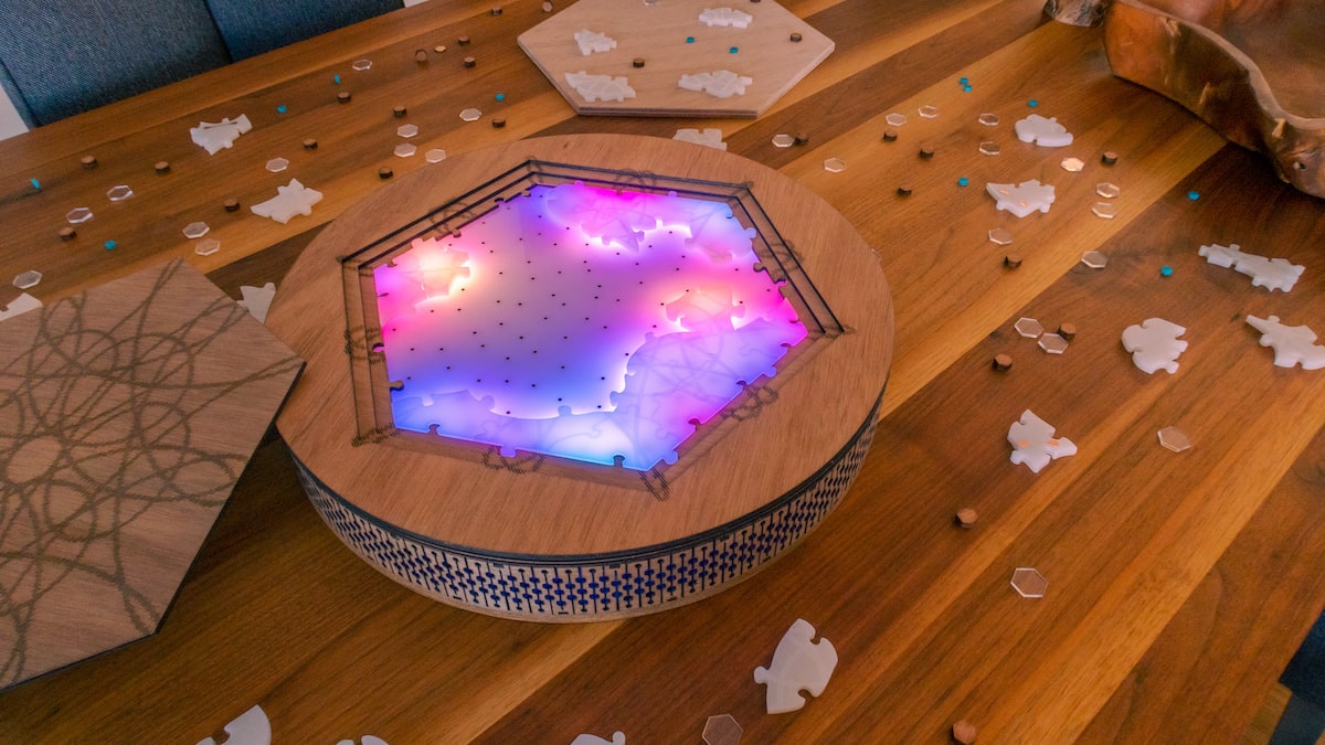
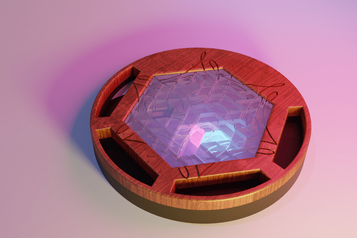
I’d already been thinking of a possible final project since September and one idea had stuck in my head. I wanted to create a jigsaw puzzle where placing each piece correctly would spark a mini light show.
I love doing jigsaw puzzles. It’s a great way from me to just zone out for a bit. It’s probably my math side, but I love how there’s only one correct solution to a puzzle, consisting of many tiny correct solutions (the placement of each piece), and if you try hard / long enough, you’ll find it.
Many people enjoy the feeling of clicking / pushing each piece into a puzzle, me included. For my final project I want to make the act of puzzling and placing each piece correctly even more fun and exhilarating for any puzzle enthusiast.
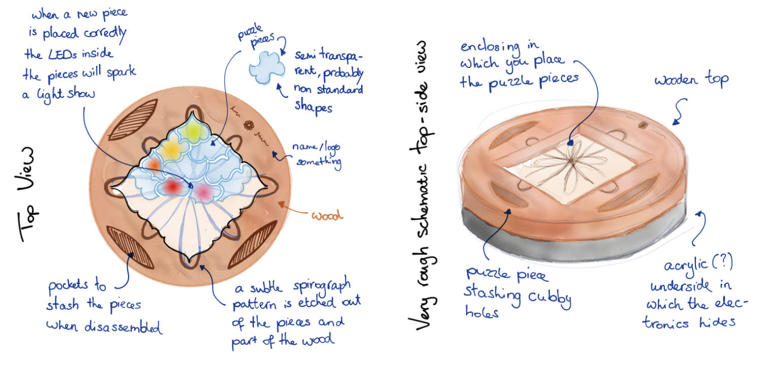
I created the sketches above on my iPad Pro and explained how I basically had no idea how I should approach the electronics. Where should the lights go? How would I know if a new puzzle piece was placed? But that was fine, Henk and others told me this was doable, and that I would slowly figure it out with the new knowledge I’d gather in the coming weeks.
You can read about the ideas that I had, the questions I still faced and some other possible project ideas on my full write-up here.
Week 2 | Computer-Aided Design
Also known as CAD. During this week I was introduced to the concept of Computer-Aided Design software with which the most intricate 2D and 3D models can be designed. Our task was to try out as many software tools as possible and create a rendering of our final project.
I’d never used any kind of CAD tool before, so I had lots to learn about how to even think about making 3D models (that aren’t just simple spheres or cubes). We got some good hands-on tutorials from instructors in different labs at the start. With that it was thankfully fairly easy to get the basic hang of, and I ended up trying Fusion 360, OpenSCAD, xDesign, Antimony and SolidWorks.
Using Blender I also made a nicer rendering of my favorite 3D model.
Eventually I gravitated towards Fusion 360 the most in terms of ease-of-use and used it for most 3D modelling in the weeks afterwards. Too bad that we only have a 1-year free license as students (but thankful that we had it in the first place). I haven’t used the open-source software FreeCAD, but that might be the tool I move to once the year is up.
You can read about all the CAD software tools that I used, and how easy or frustrating they were to work with on my full write-up here.
Week 3 | Computer-Controlled Cutting
The first machine week! Lasers! I was really excited about learning how to make things with a laser cutter. Our assignment was to make a parametric construction kit, using cardboard, which can be assembled in multiple ways while accounting for the lasercutter kerf. The kerf is the tiny, tiny section of material that the laser burns away, and it makes all the difference in materials fitting snug, or too loose if you don’t account for it.
After an online exploration to get inspired, I decided to make my own designs for Archimedean Solids; a 3D shape made from 2D surfaces (this is not the correct way to say it, but it’s easiest to get). A cube is a common example. For Archimedean solids you use a mix of different shapes, such as hexagons and squares.
I saw the new online tool Cuttle come by as an option to create 2D designs. Partly JavaScript, partly coding, partly drag-and-drop, I loved it! Cuttle is being actively developed and improved and I would highly recommend to check out if you’re going to make 2D designs for a (laser) cutting machine.
After some simple tests, and after having to re-make the connector pieces between the shapes three times because I got the math wrong at first, I created 5 different polygon shapes; a triangle, square, pentagon, hexagon, and octagon. With these I could create about 6 different “spheres”
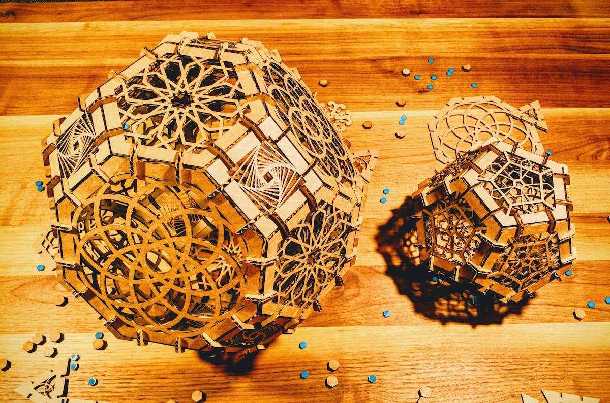
The truncated cuboctahedron and dodecahedron from the image above have now taken a spot on our (wooden) dining table. I was truly amazed how precise the laser cutter could be, how small the lines could become in the cardboard, and how cool the result could look, even in material usually only used for packaging. This was definitely one of my favorite weeks. Also because I’m really a prototyper. I love to iterate and update/perfect designs. The ease and speed of the laser cutter made it really great for fast iteration.
You can read about the whole design process and photos all of the final Archimedean Solids that I built on my full write-up here.
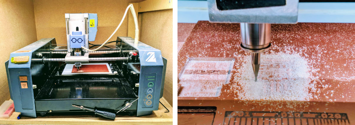
Week 4 | Electronics Production
The first electronics week! I was so new to all things electronics that I basically only started understanding what I did weeks later. I learned how to produce my owb PCB, a printed circuit board. Not to design it yet though, but to create one from an existing design. I learned how to operate a tiny milling machine that uses a 0.4mm thick mill that would mill out traces from a copper plate. I learned how to solder really tiny electrical components onto it (and how shaky my hands are, haha).
At the end of this week I actually couldn’t tell you what the boards should do that I had created. But that is part of the setup of the weeks. It’s just too much to teach you how to create a PCB and teach you the basics of electronics in one week. It was a little frustrating in this week, but I understood the reasoning.
In general I liked the setup of the weeks; it continued as machine week/electronics week/machine week/electronics week/… until about week ±17, giving a good diversity. Getting to mess around with electronics and programming, and getting to take a step back from code and bugs to muck about with machines and other materials a week later.
You can read about using the milling machine, soldering, screwing up, and ending up with a working PCB on my full write-up here.
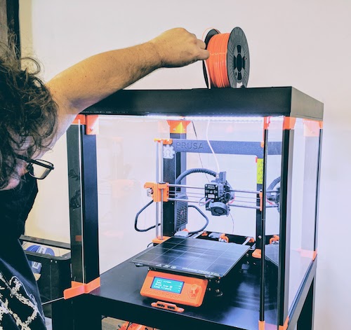
Week 5 | 3D Scanning & Printing
My very first experience with 3D printers! We had to create a design and print something that could not have been made subtractively (e.g. by a milling machine that only removes material).
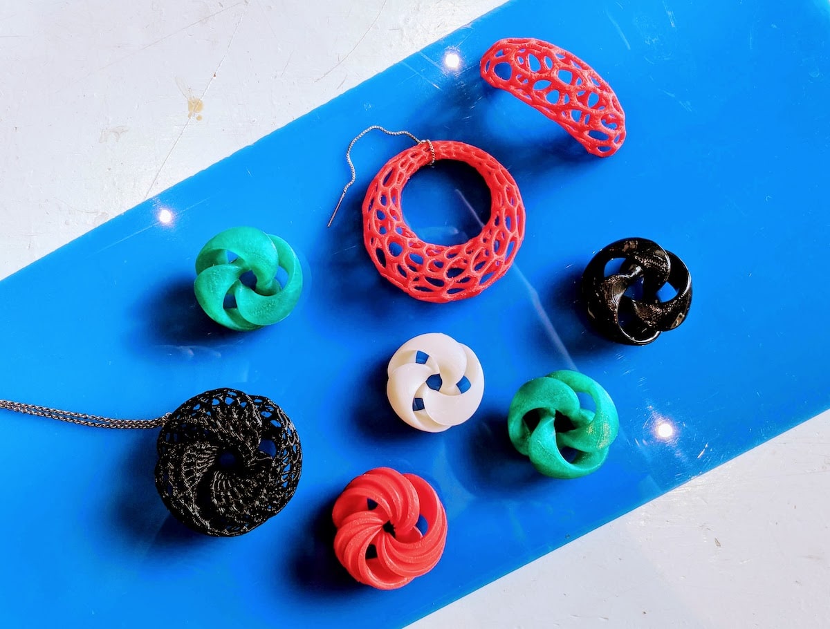
I was quickly drawn to making jewelry (we had to make something tiny, since 3D printing just takes so damn long) and to use mathematical surfaces as my designs. Being very inspired by the amazing collections of Nervous system.
This time I made my design with Blender simply because I could find a good tutorial to do it in a tool very similar to Blender that was a great start.
I learned that even the tiniest extrusion from the filament-type 3D printers we had at the Waag (the most common, where a tiny thread of filament comes from a nozzle that layers the design slice by slice) creates visible lines / slices. Not something that you want visible in something delicate like jewelry. I did learn from what my fellow students made, and how I used the machine in later weeks that it’s brilliant for making custom useful items, such as a box that fits exactly around your electronics.
Because I was trying everything I could think of to make a piece of jewelry that looked smooth I ended up with a whole collection, haha. But I’m quite happy with some pieces, especially the earrings and necklace pendant, which I’m wearing often these days.
I was so busy with the printing that I did the most simple thing for the 3D scanning that met the course requirements, haha. Scanning a tiny Pikachu nano-block statue.
You can read about every step in the design and every (failed) print I made on the 3D printer and see the results up close on my full write-up here.
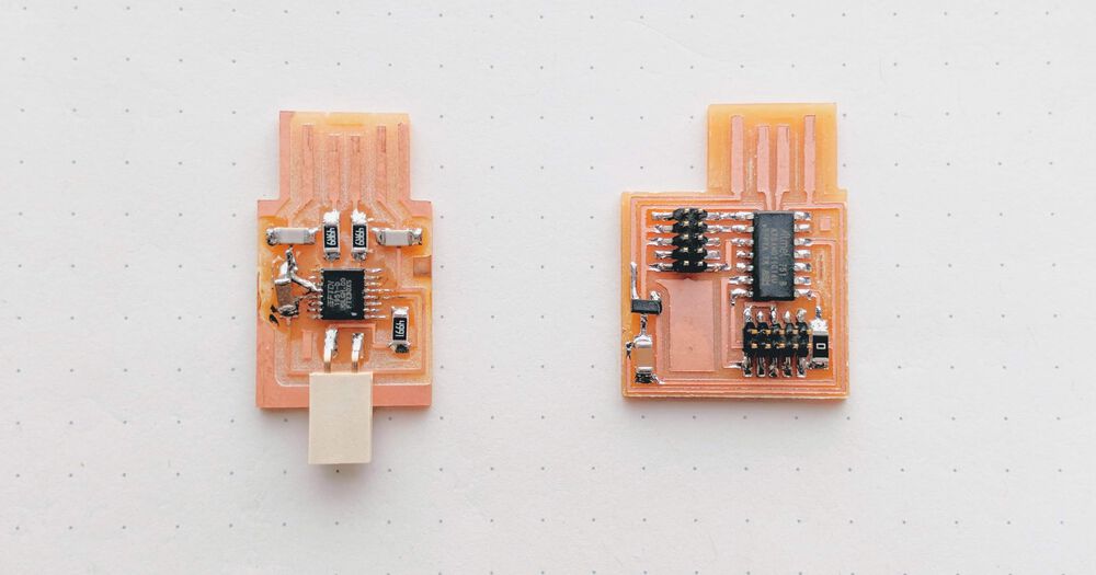
Week 6 | Electronics Design
During this week we took the electronics production process one step farther towards the beginning; we learned how to create the design of a PCB. Not yet how to figure out what electrical components are required, or what should be connected to what. Instead, we started with a so-called schematic from Henk, and learned how to lay out all those components using a software tool.
We also learned the basics of components such as resistors, capacitors, and how to use a multimeter to measure voltage, resistance, continuity and more.
I definitely understood why it takes a week to wrap your head around a PCB layout tool such as KiCad. There are a lot of steps in the process to make sure your final design will have connected the right components, without creating short circuits.
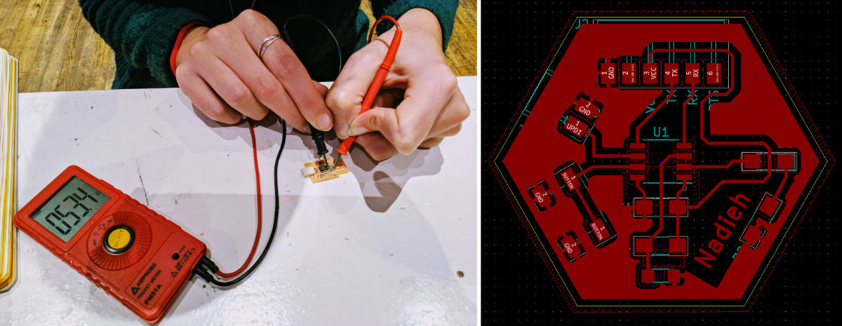
At the end of the week it was time to test the board, to load a tiny (pre-written) program onto the microcontroller at the heart of the board. At the start I had truly no idea where to even start with that task. How do I even get a program on a microcontroller?! (apparently that’s what those tiny boards I made two weeks earlier were meant for!) I came to the lab and Henk explained and showed the process, which was not that complicated, but not something you just figured out on your own. Thankfully it didn’t work on my board. I’m saying “thankfully” because it’s when you make errors that you learn the most, and I had much to learn here. I figured out the issue after a few hours and managed to fix it.
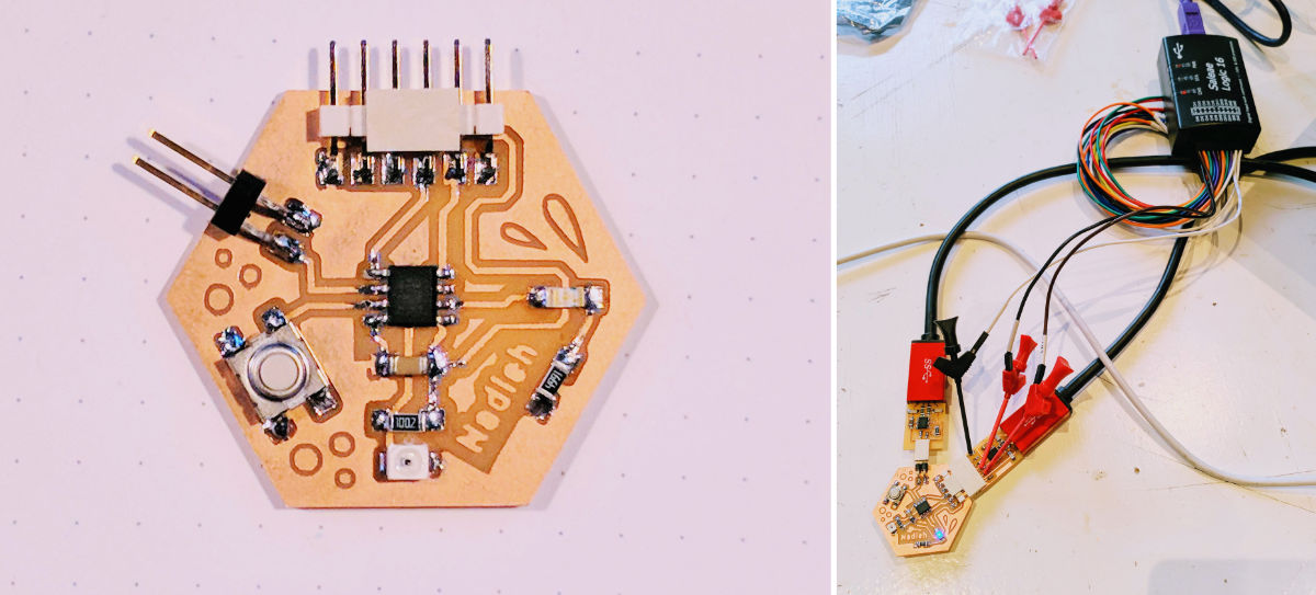
This was something I had to get used to. When I have bugs in my dataviz code I know it’s my code (or a browser bug). However, now that I’d made my own electronics it was also quite likely there was something wrong with the hardware; a broken trace, a burnt-out microcontroller. I’ll be honest, it could definitely get frustrating at times, but it was also quite rewarding to finally figure out what the issue was, to understand it.
You can read about what is needed to design a PCB and how to test it afterwards on my full write-up here.
Week 7 | Computer-Controlled Cutting
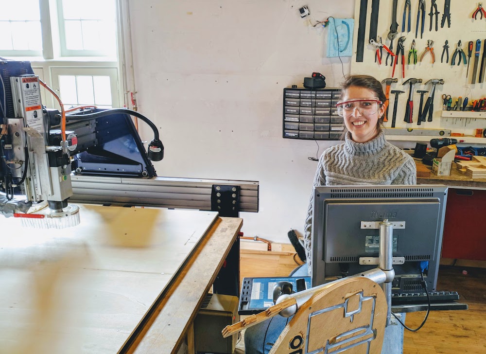
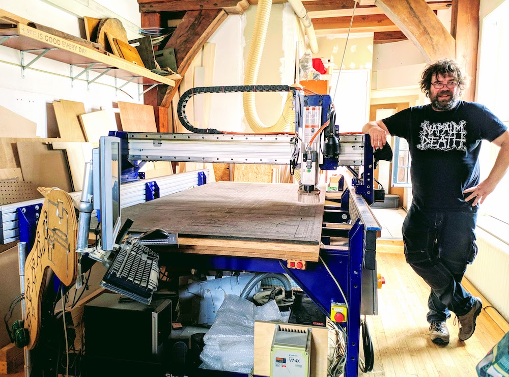
The “Make Something Big” week! We each got a wooden plate of 250cm x 122cm big (quite big!) and I chose mine to be 9mm thick. We would be using the big CNC milling machine to mill out wooden shapes that could be put together to create something, well, big.
Since this was potentially the most lethal machine in the lab the focus of this week was on safety, going slow. We had a window of 3 hours each to use the machine, and that one sheet of wood. There was no room for iteration this week. Henk therefore asked everyone to make something fairly simple.
After another online search for inspiration I saw a gorgeous wooden lamp using slices of wood, like the ribs of those tiny wooden T-Rex skeletons. I wanted to recreate my own version of that idea.
I ended up using the python plug-in from Fusion 360 to be able to create perfect mathematical shapes that changed along the length of the lamp. However, it was not an easy plug-in to work with so I wouldn’t actually recommend it σ_σ
I may look a bit complex, but it was really easy in terms of putting together; each “rib” would only need to be placed inside one long “spine” running along the length of the lamp, not much that could go wrong construction-wise.
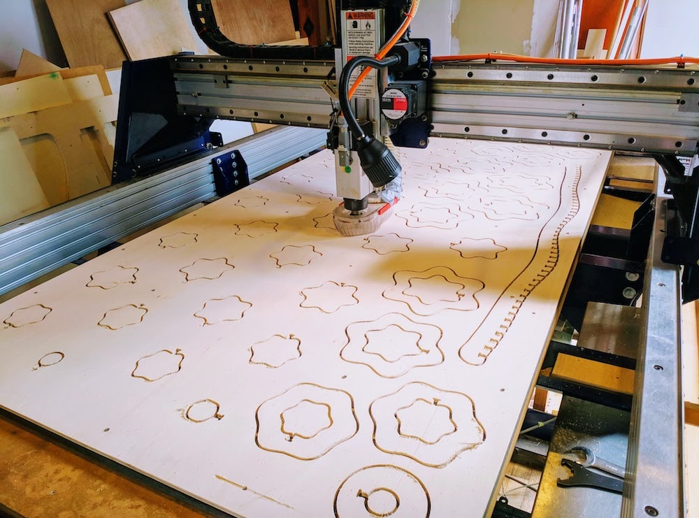
The milling all went smoothly thankfully, but I did have to sand for nine bloody hours before each slice was looking good enough (O_O) After placing an LED strip along the bottom of the spine I was really happy with the end result.
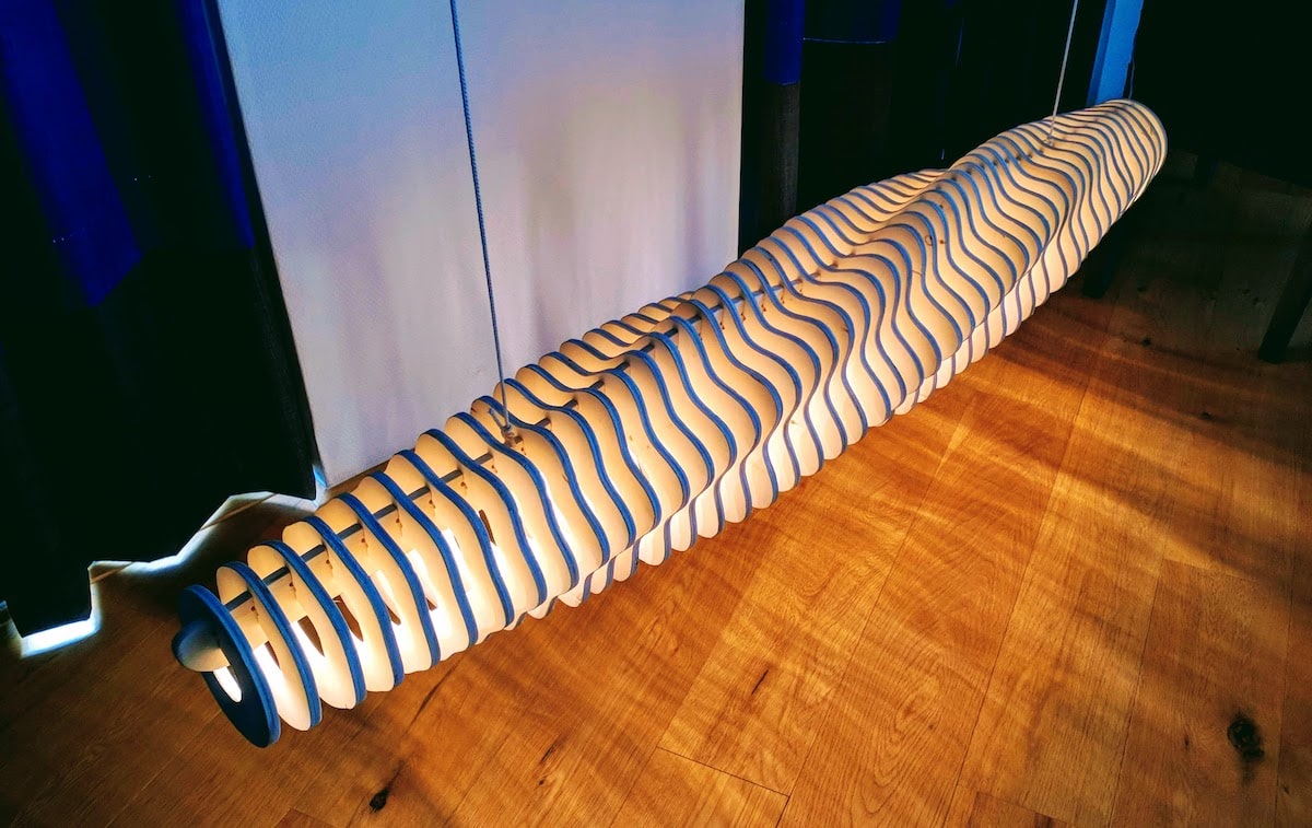
It took 10 more weeks before I had figured out, and created, the electronics (being able to turn it on/off/dim using Google Home) and how to actually hang it from the ceiling, but it’s now hanging above our dining table (ノ◕ヮ◕)ノ*:・゚✧
You can read all about the frustrating design process, how to prepare for a milling machine and the fun of sanding on my full write-up here.
Week 8 | Embedded Programming
This week we learned how to write a program for a microcontroller on a PCB. It was basically the first true programming week. I’ll be honest, if you’ve never programmed before, this wasn’t easy. Programming became an integral part of the coming weeks. From our group of 8 students, I think 2 had good programming experience and 1 or 2 were a little familiar, the rest was completely new. Over the weeks the most frustrating moments I saw from those people had to do with programming. However, the ultimate delight when something suddenly worked reminded me of my own first computers programs (in C++) during my Astronomy years.
We all adjusted what we programmed to our skills; those with experience did more complex things (generally) and those that were very new, stuck with simpler programs. Henk had explained this to me at the start of Fab Academy. His goal was not to get all students to the same level, but to push each to expand on their current level, wherever that may be and in whatever topic (e.g. in electronics, machinery, etc.).
We used the board we created two weeks before to program during this week. We all gravitated towards using the Arduino IDE as the main tool to program with. Throughout the week I worked through several examples; from a blinking and fading LED, to pressing a button, and using a phototransistor as an input to make the LED blink faster or slower.
We also played a little with several other “commercial” boards (pre-made), such as different Arduino boards. I was happy to finally learn what an Arduino was and what you could do with it (I seriously never looked into this before, I only knew the word).
You can read about my tests and the code that I used on my full write-up here.
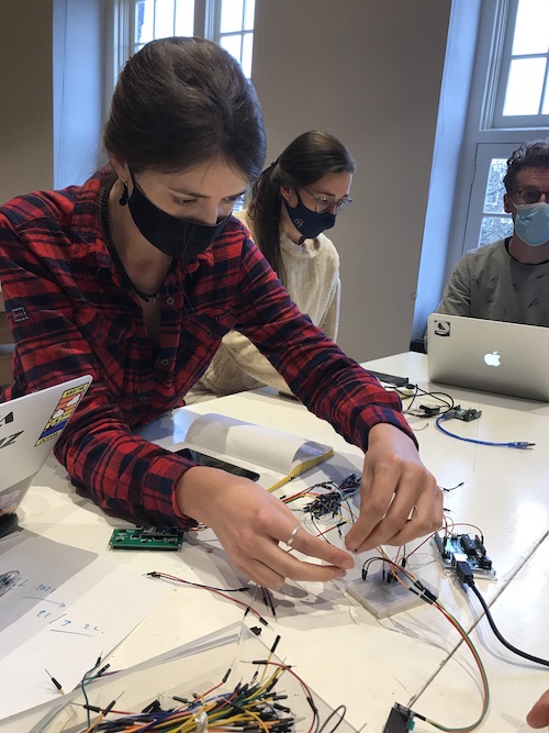
Week 9 & 10 | Mechanical & Machine Design
These were two crazy intense weeks! This was one big group assignment where we had to create a machine! Something that used tiny motors, such as stepper motors or servo motors.
We made two teams and our team of four ended up making a folding lamp that reacted to light; when it is dark the lamp folds open and wants to show how beautiful it is with lights. However, when it becomes too bright, and the lamp can’t be the brightest in the room anymore, it becomes sad and closes.
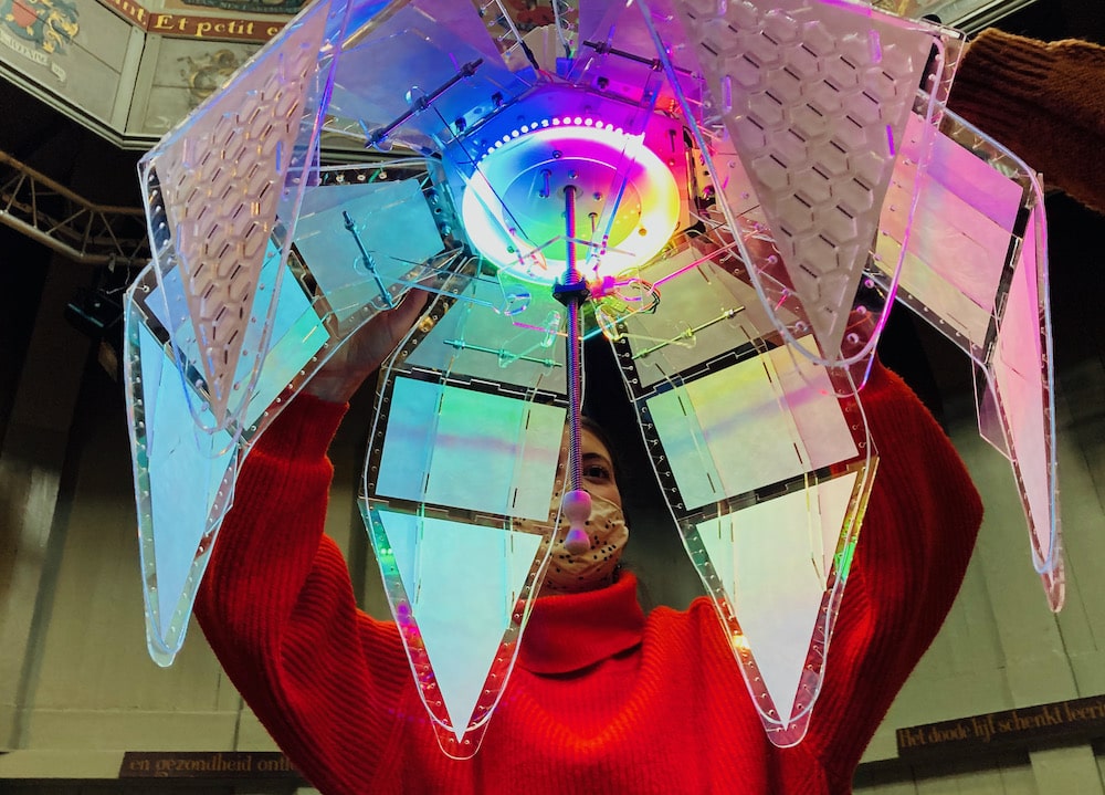
Together with teammate Nicole we figured out how the lamp should fold and how a central motor would make that possible. I created the design for the petal shapes with Fusion 360 and had them cut from acrylic with the laser cutter. The lights were also fun, where I worked closely together with another teammate Loes to incorporate it into the lamp and have her light programming work with the opening and closing of the lamp.
Below is the presentation video of the creation and function of our lamp, Flo, created by teammate Douwe Schmidt.
You can read all about how these became the most intense two weeks of the whole Fab Academy for me, designing the lamp’s exterior and programming it, on my full write-up here.
Week 11 | Input Devices
Going back to electronics again. This week we focused on input devices, anything that responded to an outside something and would relay that result back to a microcontroller. From light to sound, touch, magnetism, distance, switches and more.
This was also the first week where everybody started diverging and generally investigated input devices that they might be able to use for their final project. For me that became a research into switch-like devices. I needed to somehow capture when a puzzle piece was being placed, to know which puzzle piece locations were occupied and which still open.
It was also finally time to fully design my own PCB. Even figuring out which components I required and how it all should be wired. It felt quite daunting, but with lots of research during the weekend, looking back on my previous electronics weeks, and documentation from previous students to learn from, I realized I was indeed ready for it.
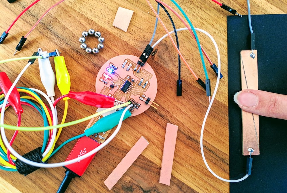
I ended up choosing to investigate a magnetism sensor, a simple switch, and a capacitive touch sensor.
You can read about all the input tests that I did and how I designed my board on my full write-up here.
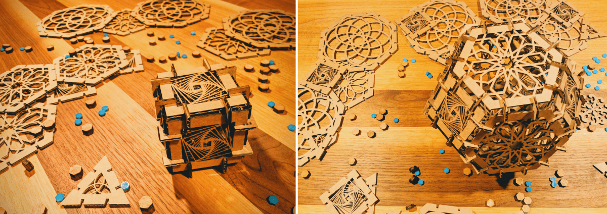
Week 12 | Molding & Casting
This wasn’t really my kind of week, but I knew that going in to it. I’m just not one for working with materials that get messy, and molding and casting is all about messy. For this week we had a small block of machineable wax from which we had to make a three-way mold (I won’t go into the details of what that is exactly).
With the idea being that in the end you could quickly create many of the same shape, I figured I might as well make a puzzle piece that would fit in itself. Usually I would spend the whole weekend on my design, but since this wasn’t quite my thing, I made this one in an evening and created the mold on Friday already.
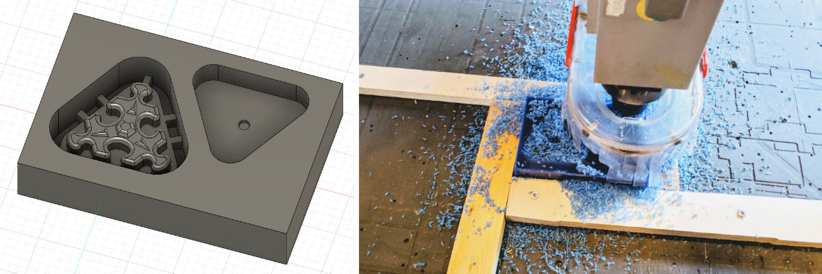
I then poured (purple) silicon into the wax. These purple sections became the final mold that I could use to make my puzzle pieces with from yet other materials. Sadly the milling machine had been set too rough, too fast, on the creation of the wax mold, which resulted in an extremely crude result. So bad that the final puzzle pieces didn’t even truly fit into each other. Thankfully, I’d bought a bunch of glitter at the start of the week, which made it a bit more fun again, and also embedded an LED into one piece for the fun of it.
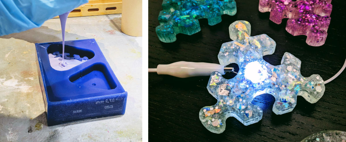
After trying several batches of transparent casting material with a crazy amount of glitters I had a tiny collection of puzzle pieces.

You can read more about the design and molding and casting process of these puzzle pieces on my full write-up here.
Week 13 | Output Devices
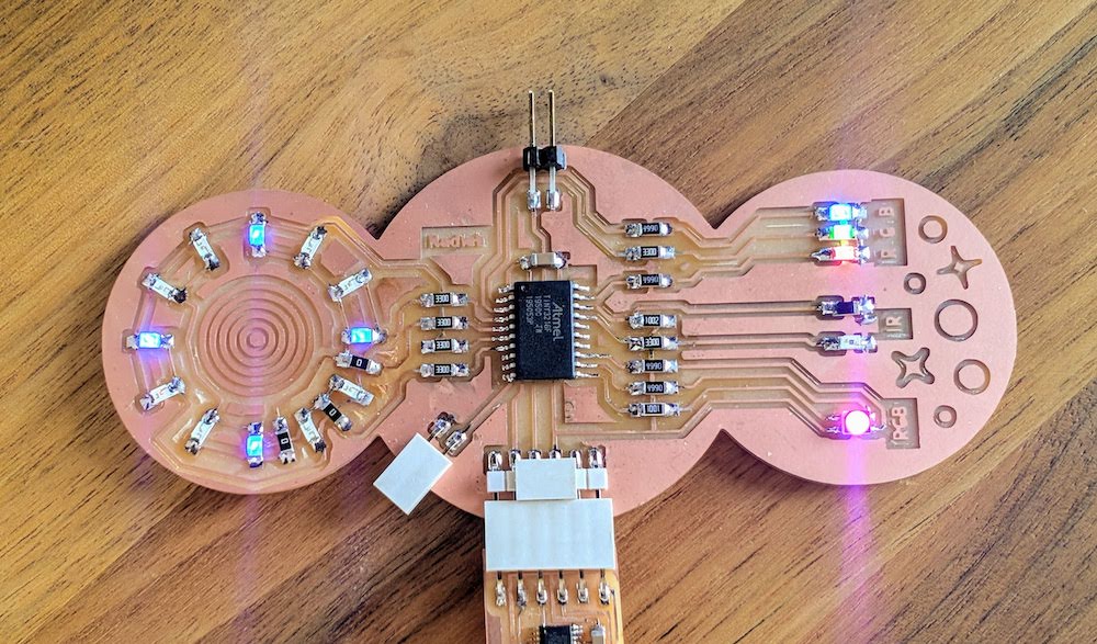
A logical next step in electronics after the Input Devices week before. This time we dove into the devices that a microcontroller could act on, things that show an output, such as LEDs turning on/off and motors moving. I stuck with lights. I’ve always been fascinated by the self-made projects that incorporate lights somehow. It’s a big reason why I also wanted to have lights in my final project.
I designed and made a PCB that used an RGB LED, a infrared LED and infrared phototransistor, and charlieplexing (using LEDs with fewer connections back to the microcontroller than the number of LEDs, quite fun to slowly figure out).
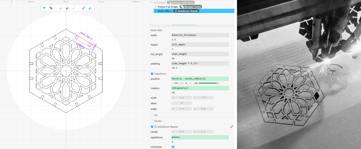
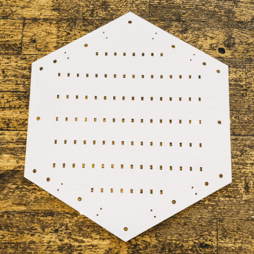
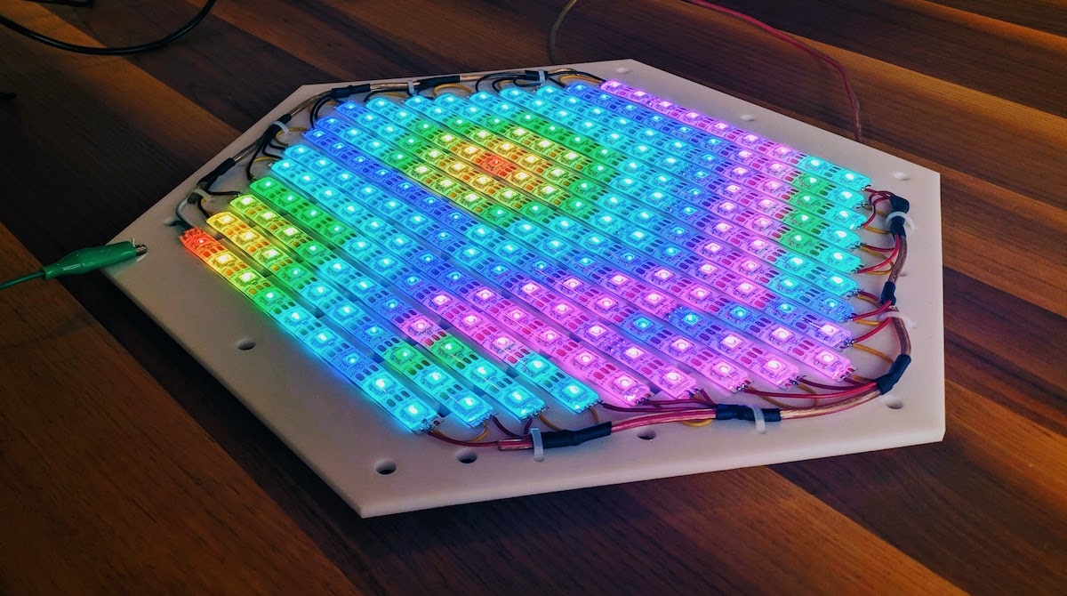
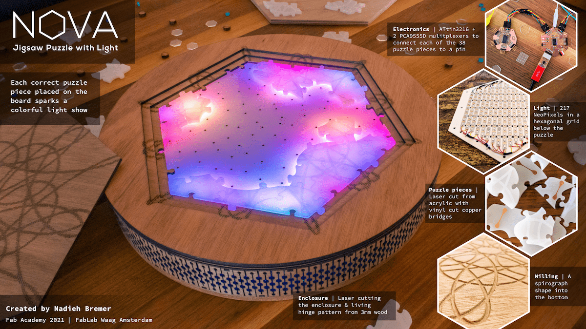
However, my main goal this week was to create the big grid of lights that would go underneath the puzzle for my final project. A grid consisting of 217 separate NeoPixels, which are a wonderful type of LED where each LED can be separately programmed, but the whole only requires one connection back to a microcontroller.
Henk had bought a 5 meter strip consisting of 300 NeoPixels. Using Fusion 360 I’d drawn out my grid. After laser cutting the base from a white acrylic plate a very tedious work began where I had to cut up the 5 meter long strip and turn it into a hexagonal grid, involving lots of soldering.
Thankfully, after I (shaking from nerves) reconnected the NeoPixels to power after 8 hours of cutting and soldering it all still worked!! (๑•̀ㅂ•́)ง✧
Even though the 5 meter long string was now turned into a hexagon grid, it was still connected as a long string. Programming the 1D string to show 2D-like visuals was still a bit of a mind-f*$k. But after several frustrating hours I eventually had some really simple things working by the time the week ended.
You can read all about how I created my light-board, and even more so, the grid of 200+ NeoPixels on my full write-up here.
Week 14 | Networking & Communications
By now we’d gone through all the machines in the lab and therefore continued with more topics related to the electronics side. For this week we learned (a lot more) about different protocols with which to send information between boards, creating a network. Where one device is often the one in charge and the others are following tasks being sent to them and/or possibly sending information back to the main hub.
I used this week to create the main PCBs for my final project. With what I’d learned over the past weeks I had finally gotten a grasp on how I wanted to do the electronics. I’ll leave it at that for the details, but it came down to requiring 3 hubs in a way, which had to communicate, thereby being a good fit to combine with this week.
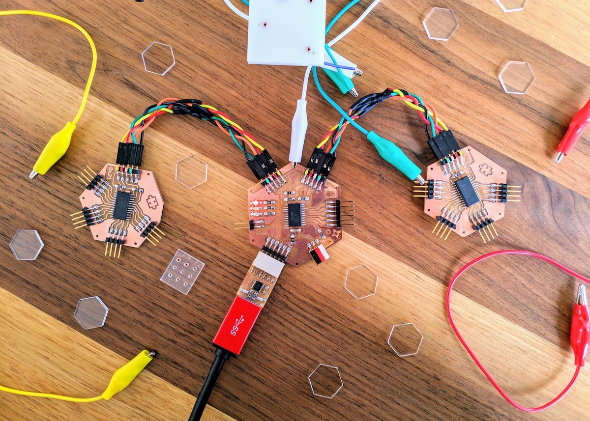
You can read all about my process of creating these PCBs and testing puzzle connections on my full write-up here.
Week 15 | Interface & Application Programming
This was basically my “bubble” week, this was extremely close to my day job. The tools explained included python, JavaScript, D3.js (and dozens more). Our assignment was to write an application that connects with an input/output device that we had made before. Basically how to get something out of or in to a PCB using something visual on a computer screen.
I figured that I’d never truly tried to visualize just one changing number. I therefore grabbed my very first hexagonal PCB and visualized the value coming from its phototransistor (running between 0 - 1023), using several browser-based tools; D3.js, HTML5 Canvas, WebGL, and p5.js.
Being familiar if not comfortable with these tools the most difficult part for me this week was to connect a PCB to my laptop and read data from it. Thankfully there were (naturally) Node.js packages and python packages.
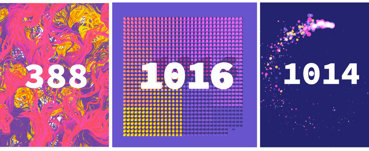
I decided to not dive into new territory (such as AR or VR) for the topic of this week, but spend half on making an example with four of my favorite dataviz tools, and spend half on my final project; soldering and wiring up all the electronics.
You can read more about how I created these data visualizations on my full write-up here.
Week 16 | Wildcard Week
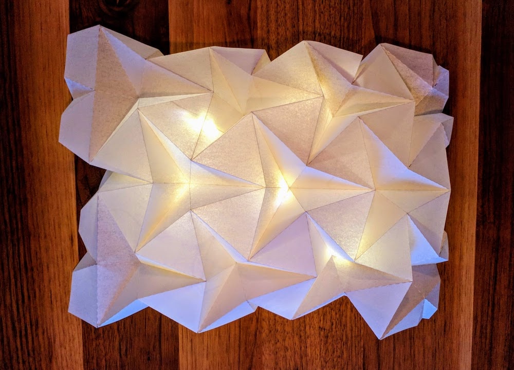
As the name suggests, this week we were free to decide what machine or process we wanted to explore. The lab needed to have the machine for it of course. For example, I really hoped there was a knitting machine, but although it had been ordered ages ago, it still wasn’t delivered (think KickStarter issues). Working with composites is typically done at the Waag. Since that is an even messier process than molding and casting I knew it wasn’t a good fit for me. However, I saw that origami was also an option!
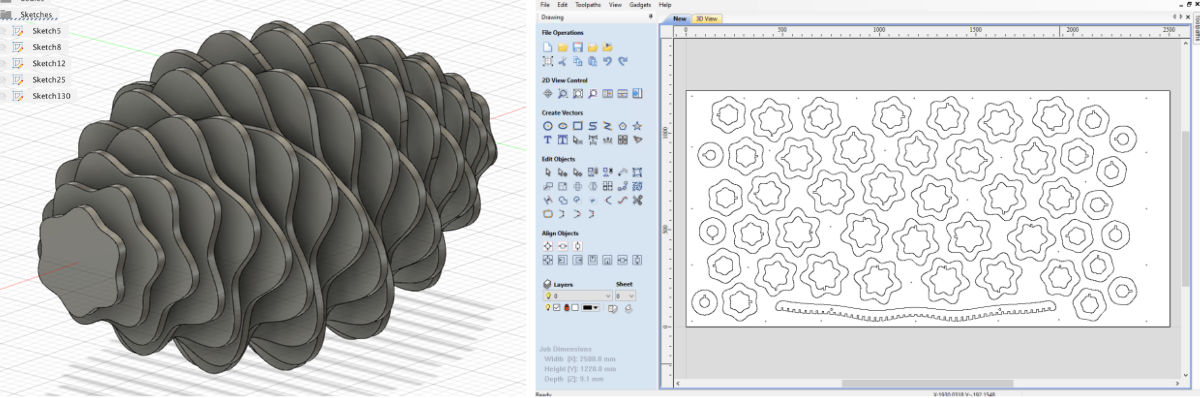
I really love origami, not quite the animals and objects, but more the mathematical surfaces, tessellations and spheres. I wanted to try and use machines, the laser cutter or vinyl cutter, to pre-etch lines into paper that could then easily be folded into tessellated areas, drastically reducing the time it would take to produce them.
It took dozens of failed experiments, but I eventually found a technique that made even quite sturdy paper easily pop into tessellations that had taken 1-2 hours for me to completely fold by hand.
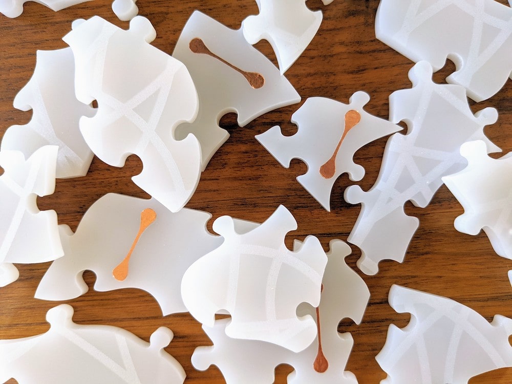
As before, I was also working on my final project during this week, focusing on making the puzzle pieces from milky-white acrylic.
You can read all about the many origami tests, and many, many failures, I went through on my full write-up here.
Week 17 | Applications & Implications
By this week you’re basically working full-time on your final project. The individual weekly assignment comes down to describing the final project in more detail, answering questions such as “what has been done before?” and “what techniques are you using?”, something that could be done in an hour.
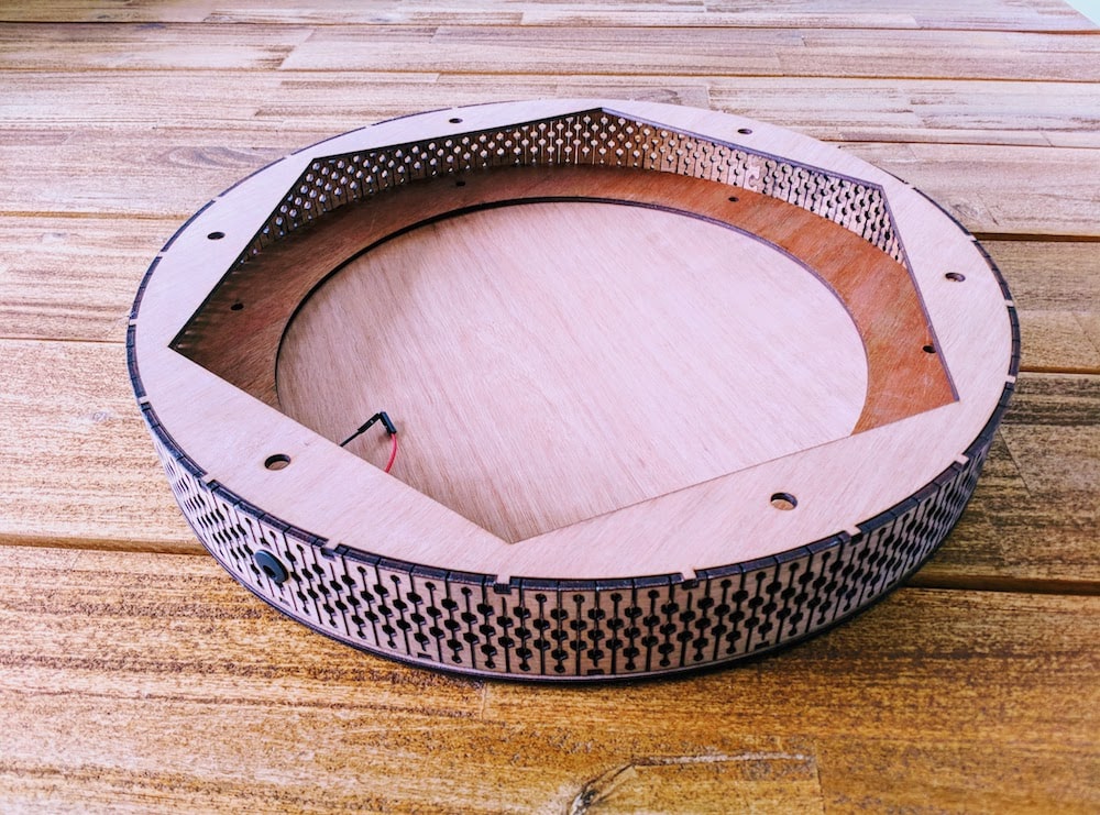
For the remainder of the week I worked on creating the wooden enclosure, using the technique of a living hinge to bend wood in a circle. I really loved exploring this technique (also made earrings) and seeing how wobbly and bendable wood, plastic and even acrylic could become.
You can read the plan and explanation I created for my “masterpiece” on my full write-up here.
Week 18 | Invention, Intellectual Property & Income
This week you’re spending all your time on the final project as well. The class lessons will be focused on taking your final project to the next step, turn it into a business, and what you need to consider in terms of possible patents and licenses.
For the individual assignment you’re asked to decide what license you want for your final project and explain how you’ll be sharing the work (online). If you’re not planning to go any further with your final project after Fab Academy, like me, like most, this is easy to figure out and write.
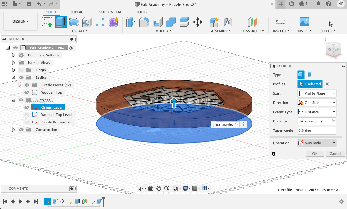
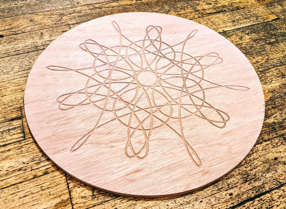
For my final project it took me several days this week to experiment with different machines, and different woods, to create a wooden top (and bottom) plate for the enclosure.
You can read the license that I choose on my full write-up here, but it’s truly not that interesting.
Week 19 | Final Project
This is the final week! No weekly assignment, but one more week to finish that final project before the presentations begin. I used this week to program my puzzle now that the physical “puzzle box” was finally complete. To make sure that when a puzzle piece is placed, the LEDs below it light up, and to create several fun animations that occur when you plug in the power, place a piece, and of course, place the last piece.
Week 20 | Final Presentations
With ±200 global students there isn’t much time to present. It therefore goes quite streamlined, while a slide and short movie are used to show the project.
You have to make a slide that conveys the final project and main techniques and electronics used. Below you can see my final slide.
And even more important is the presentation video of ±1 minute that shows the final project and its creation process. I have to stress that it’s very important to show that it actually works! and it was kind of funny to see how many students didn’t actually show this ┐( ̄ヮ ̄)┌ Not because it wasn’t working I think. Instead because each student has been too close with their project and everything seems so logical. But not for a person seeing it for the first time.
Below is my final presentation video:
Everybody got ±3 minutes of “presentation time” that starts with Neil showing your video to everyone watching in the call. Afterwards he’ll ask some questions, and/or make some remarks on how it might be improved. The 3 minutes isn’t completely strict. Some projects are clear as day and less time is used, with other projects there are more questions and it goes a little over the alloted time.
I was nervous for sure, but not in a “I might fail” kind of way. Neil is very friendly, but he will tell you if your project does not meet all the requirements, telling you what you should improve before you can graduate. Often it was as simple as “add a few more seconds to the video showing the full project working/moving/updating”. The general idea is that you can’t fail, you’ll just be graduating at a later time if you can’t fulfill all the requirements right now.
You can find an endlessly long write-up of every facet that went in to designing, building, and programming my final project on this page
My Overall Experience
I’m really happy I participated in Fab Academy! It’s been a very long time since I’ve learned so much in a few months. I still remember thinking in week 10 (the “Machine week” group assignment) looking at our folding lamp, that just 10 weeks before I would’ve had truly no idea how I could’ve made that machine, let alone programmed it, and here I was, looking at a lovely folding lamp with light effects and all.
There were definitely frustrating things; when your PCB isn’t working and the errors are so vague you have no idea what might be causing it, when you have a certain idea that’s beyond the machine’s limit. And not every aspect of every week was something I truly enjoyed. Designing PCBs wasn’t a favorite of mine, where you have to figure out what components are needed. I still feel like I’m missing too much knowledge about the electrical components to feel comfortable with it. In that sense, in the future I see myself working more with commercial boards instead. However, others really liked designing and creating a PCB, so it’s all personal.
However, those frustrations were nothing compared to the fun and excitement of learning and making cool sh*t each week! I now have (another) unique ceiling light in my house, several cool trinkets to liven up my room, and a bunch more earrings and other jewelry that I’m really happy with.
I still have no idea how to bring this knowledge back into my work. However, I’m going to try and make time to work on some personal dataviz related projects involving fabrication processes to put in my portfolio, and I’m really looking forward to that.
Wrapping Up
I hope this blog has helped to explain what the Fab Academy is, how a typical week looks, and what you’ll be doing in the different weeks. I hope it will help those thinking about whether or not they want to apply to decided one way or the other. And for those that apply, good luck and have fun, you won’t regret it! 。^‿^。
Random final comment | I wonder how many of the people I told “I’m studying at the Fab Academy”, were thinking it was short for “Fabulous Academy”, and then probably trying to think of what the heck you’d be learning there (*^▽^*)ゞ Or am I the only one that’s watched too many Absolutely Fabulous in the past and instantly connects “fab” with “fabulous”, LOL.